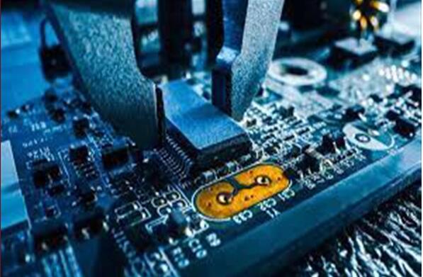
SMT Printed Circuit Board Assembly

Descripció del producte
china smd assembly and manufacturing is the process of connecting components to a printed circuit board (PCB) to create an electrically functional system. It involves soldering components to the board, such as integrated circuits, resistors, capacitors, transistors, and connectors. The custom PCB assembly is then tested and inspected to ensure that it meets the manufacturer's specifications and requirements. This process is essential for the functionality and reliability of the end product. PCB assembly including prototype pcb and pcb assembly requires a high degree of precision and accuracy and is often done by automated machines to ensure quality and consistency. It is the basis for many electronic products and is used in a variety of industries, from consumer electronics and medical devices to military and industrial applications.
What is the PCB assembly process?
1. PCB design: Create a design for the PCB, including component placement, trace routing, and other specifications.
2. PCB fabrication: Use the design files to produce the PCB assembly board with the desired components.
3. Component procurement: Obtain the components needed for the PCB assembly.
4. PCB inspection: Inspect the PCB for any defects or errors before assembly.
5. Component placement: Place all components onto the PCB board using automated machines or manual placement.
6. Soldering: Use a soldering iron to securely attach components to the board.
7. Reflow soldering: Use a reflow soldering oven to attach components to the custom circuit board assembly board, this is used for high-volume production.
8. PCB testing: Test the PCBs to ensure they are working correctly.
9. PCB packaging: Package the PCBs into their respective cases or containers.
What is the difference between PCB fabrication and PCB assembly?
Custom PCB fabrication and custom PCB assembly are two distinct processes in the manufacturing of printed circuit boards. PCB fabrication is the process of creating a printed circuit board from raw materials such as copper, fiberglass, and other necessary components. This process typically involves etching the copper onto the fiberglass substrate, drilling the necessary holes, plating the holes, and applying solder mask. PCB assembly is the process of soldering components onto the printed circuit board. This includes soldering components such as resistors, capacitors, chips, and other electrical components onto the PCB assembly board. PCB assembly also involves attaching connectors and other components onto the board. Both processes are necessary for creating a functioning printed circuit board.
FAQs of PCB Printed Circuit Board Assembly
Q
What necessary information do you think you need to know in order to assemble a PCB?
A
In order to assemble a PCB, you need to have a good understanding of electrical engineering, including circuit design and component knowledge. Additionally, you'll need to know the type of components to be used, their values, the board layout, the connections between components, and the order in which components need to be added. You'll also need to know the type of soldering technique to use, the types of soldering materials and tools required, and the safety precautions to take. Finally, you'll need to understand the testing procedure to ensure the board is functioning correctly.
Q
What material is used to assemble components in PCBs?
A
The material used to assemble components on PCBs is typically a combination of different metals, including copper, tin, and silver. Copper is the most common metal used, as it is the most conductive and durable. Tin is used to cover the copper traces, providing protection and helping to reduce the risk of short-circuiting. Silver is often used as a final coating to provide additional protection and increase the conductivity of the board.

